Truly two-dimensional objects are rare. Even a thin piece of paper is trillions of atoms thick. When physicists do succeed in producing 2D systems, quantum interactions can lead to new phenomena and Nobel prizes. Two examples: graphene---single-atom-thick sheets of carbon atoms---has unique mechanical, electrical, and optical properties; and two-dimensional electron gases (2DEG)---planar collections of electrons supported at the interface between certain semiconductors such as gallium arsenide---allow the observation of such emergent behaviors as the quantum Hall effect and the spin Hall effect.
A relatively new frontier for studying 2D matter is provided by planar collections of electrons at the surface of transition-metal-oxide (TMO) materials, in which high electron densities give rise to interactions that are stronger than in semiconductors. Consequently it is more accurate to refer to the TMO electron ensemble as a 2D liquid rather than as a 2D gas. Scientists hope to find exotic emergent phenomena in these high-density, highly-interactive electron environments.
One of the leaders in this effort is James Williams, a new fellow at the Joint Quantum Institute (JQI), where he is also an assistant professor of physics at the University of Maryland. Before he left Stanford University, Williams and his colleagues performed tests on a thin sample of strontium titanate (STO) covered over with an electrolyte gel, a material in which negative and positive ions dissociate (saltwater is a common electrolyte: Na+ and Cl- ions come apart in a water solution). Their results appear in the journal Nature Physics. The article is accompanied by a "News and Views" essay recounting the highlights of the work.
The Experiment
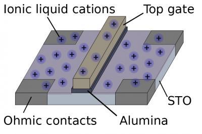
Figure 1 shows the basic setup of the work conducted at Stanford. A thin STO panel, covered by a gate electrode down the middle, is wetted by an electrolyte gel. The negative ions in the electrolyte are drawn off by an unseen electrode and can be forgotten. Meanwhile the positive electrolyte ions settle down on the STO surface, where they induce a dense 2D layer of electrons to form directly beneath. The transport of these electrons as a current can be encouraged or discouraged by a voltage applied to an overlying electrostatic gate, pretty much the same arrangement used to move currents through field-effect-transistors (FETs), one of the universal components of myriad electronic devices. In effect, voltages applied at the 50-nm-wide gate region can create a barrier cutting off one portion of the material from the other or, conversely, offering a passage from the one side to the other.
Now is the time to mention that TMO materials are versatile. They can be insulating, conducting, semiconducting, superconducting and even show signs of ferromagnetism. Williams and his colleagues at Stanford and Santa Barbara were the first to discover that bulk strontium titanate (a common TMO) that was simultaneously superconducting and ferromagnetic. Furthermore, the same material can be tuned from one type of behavior to another, usually by changing the density of electrons in the sample.
In the present experiment, the interest is in seeing how normal and supercurrents flow through tiny channels from one superconducting STO panel to another through a narrow passage. The passage is so narrow -- comparable to the size of the electrons considered in their wavelike manifestation -- that quantum effects are expected to occur.

This is a schematic of the device, which is submerged in an ionic liquid. A positive electrode (not shown) draws away the negative ions in this liquid, leaving the positively-charged ions (plus signs) to induce a dense layer of electrons in the (lavender-shaded) strontium titanate layer beneath.
(Photo Credit: Stanford University)
The size of the opening and the consequent flow of current through the barrier to the other side can be controlled by changing the gate voltage. At low voltages (and at densities of less than about 8 x 10^12 electrons per sq. centimeter) the barrier material remains an insulator. Little or no current flows. At medium voltage and density, some quantum tunneling proceeds; that is, some electron-pairs can leap to the other size. At higher voltage and at higher density (above 5 x 10^13 per/cm^2---a hundred times larger than is present in most FETs) tiny conducting zones can materialize. When some of these zones link to span the barrier, an effective channel allows superconducting currents to flow freely.
These little free-current gauntlets---called quantum point contacts---have been studied before, but not in strontium titanates. What justifies the use of the word quantum here is that the conductivity of the superconducting STO material is quantized. That is, the conductivity of Cooper pairs should only occur at certain levels, namely multiples of 2e^2/h, where e is the charge of an electron and h is Planck's constant.
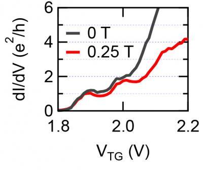
But graphs of current versus gate voltage show that the conductivity (equal to the slope of the graph at any one voltage) can also occur at multiples of e^2/h. This suggests that the electrons flowing through the tiny passage have their spin degree of freedom broken, just as electrons in a ferromagnet don't have the freedom to point in any direction but are lined up in a coordinated way. The combination of the high electron density and potent electron interactions are not seen in other materials and the quantum regime enforced by the tight passageway, might here be engendering some new kind of electron transport.
As the electron density outside the quantum point contact is increased, the material becomes superconducting and the transmission of Cooper pairs – the particles that comprise a superconducting current – through the constriction was also studied in this work. But something is missing: Cooper pairs are made of pairs of electrons with opposite spins, yet in the constriction these two degrees of freedom are not available. How then, do Cooper pairs make it through the constriction? Could this particular TMO have Cooper pairs that don't get together in the conventional way?

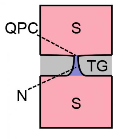
Within the top gate barrier (which is otherwise an insulator), a very narrow passageway which conducts electrons normally (N), can link the superconducting (S) panels on either side of the top gate. The passage is known as a quantum point contact (QPC).
(Photo Credit: Stanford University)
Looking for Novel Forms of Superconductivity: P-Wave Versus S-Wave
Their new experimental results are reported online in the journal Nature Physics on August 31, 2014. The authors speculate that this behavior is consistent with (but not yet proof of) of novel superconductivity, one candidate of which is a p-wave superconductor . More research needs to be done before this speculation is given a strong footing. In conventional, or s-wave superconductivity, the pairs of electrons (Cooper pairs) that constitute a zero-resistance current, are spherical in shape. In p-wave superconductivity, the pairs would look more like miniature dumbbells festooned with additional lobes.
P-wave superconductivity has not been unambiguously seen yet since the anatomy of the electron pairs is difficult to establish. But the search has generated much interest. This is because theorists believe the p-wave materials could support the existence of Majorana particles (named for physicist Ettore Majorana), which are expected to have strange properties, such as being their own antiparticles.

This is a graph showing the conductivity across the device (the rate of change of current with voltage) versus applied gate voltage. The appearance of a plateau at a conductivity value of e^2/h is notable.
(Photo Credit: Stanford University)
Source: Joint Quantum Institute