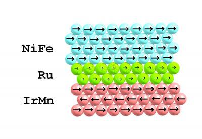
A layer of ruthenium just a few atoms thick can be used to fine-tune the sensitivity and enhance the reliability of magnetic sensors, tests at the National Institute of Standards and Technology (NIST) show.* The nonmagnetic metal acts as a buffer between active layers of sensor materials, offering a simple means of customizing field instruments such as compasses, and stabilizing the magnetization in a given direction in devices such as computer hard-disk readers. A thin layer of ruthenium (green in the cartoon) improves magnetic sensors by modulating interactions between a nickel/iron film (blue) that responds to external magnetic fields and an iridium/manganese stabilizer film (pink). The ruthenium aligns its electron spins, indicated by arrows, with the nearest layers in both films. Credit: NIST
In the NIST sensor design, ruthenium modulates interactions between a ferromagnetic film (in which electron “spins” all point in the same direction) and an antiferromagnetic film (in which different layers of electrons point in opposite directions to stabilize the device). In the presence of a magnetic field, the electron spins in the ferromagnetic film rotate, changing the sensor’s resistance and producing a voltage output. The antiferromagnetic film, which feels no force because it has no net magnetization, acts like a very stiff spring that resists the rotation and stabilizes the sensor. The ruthenium layer (see graphic) is added to weaken the spring, effectively making the device more sensitive. This makes it easier to rotate the electron spins, and still pulls them back to their original direction when the field is removed.
NIST tests showed that thicker buffers of ruthenium (up to 2 nanometers) make it easier to rotate the magnetization of the ferromagnetic film, resulting in a more sensitive device. Thinner buffers result in a device that is less sensitive but responds to a wider range of external fields. Ruthenium layers thicker than 2 nm prevent any coupling between the two active films. All buffer thicknesses from 0 to 2 nm maintain sensor magnetization (even resetting it if necessary) without a boost from an external electrical current or magnetic field. This easily prevents demagnetization and failure of a sensor.
The mass-producible test sensors, made in the NIST clean room in Boulder, Colo., consist of three basic layers of material deposited on silicon wafers: The bottom antiferromagnetic layer is 8 nm of an iridium/manganese alloy, followed by the ruthenium buffer, and topped with 25 nm of a nickel/iron alloy. The design requires no extra lithography steps for the magnetic layers and could be implemented in existing mass-production processes. By contrast, the conventional method of modulating magnetoresistive sensors—capping the ends of sensors with magnetic materials—adds fabrication steps and does not allow fine-tuning of sensitivity. The new sensor design was key to NIST’s recent development of a high-resolution forensic tape analysis system for the Federal Bureau of Investigation (see Magnetic Tape Analysis “Sees” Tampering in Detail).
* S.T. Halloran, F.C. da Silva, H.Z. Fardi and D.P. Pappas. Permanent-magnet-free stabilization and sensitivity tailoring of magneto-resistive field sensors, Journal of Applied Physics. August 1, 2007.