Iron selenide (FeSe) is an attracting superconducting material since the superconducting transition temperature (Tc) is enhanced from 8 K in bulk form toward 65 K in one-monolayer form.
However, systematic thickness dependence of electrical measurement has been difficult to address.
A team of researchers at Tohoku University's Institute for Materials Research (IMR), has realized layer-by-layer etching in superconducting FeSe films down to approximately one-monolayer about 0.6 nm using classical electrochemical reaction in electric-double-layer transistor configuration.
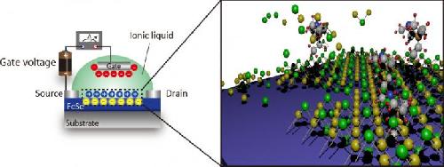 (Left) Device structure of electric-double-layer transistor with FeSe channel deposited on oxide substrate. (Right) One-monolayer FeSe is realized by electrochemical etching where Fe and Se ions are dissolved into ionic liquid. Credit: Junichi Shiogai
As the thickness of the films becomes thin, the superconducting transition temperature (Tc) is increased from bulk value (8 K) to about 40 K. In addition, the research group unveils that by combining with an electrostatic charging effect, the high-Tc transition can be induced in 10-nm thick condition (20 monolayers), which had been limited in one/two-monolayers so far.
The development of this etching technique will pave the way for the exploration of nontrivial physical phenomena in atomically thin two-dimensional films. This had previously been difficult to address by conventional methods.
This work was published in Nature Physics online on Nov 2, 2015.
source: Tohoku University