The smaller components become, the more difficult it is to create patterns in an economical and reproducible way, according to an interdisciplinary team of Penn State researchers who, using sound waves, can place nanowires in repeatable patterns for potential use in a variety of sensors, optoelectronics and nanoscale circuits.
"There are ways to create these devices with lithography, but it is very hard to create patterns below 50 nanometers using lithography," said Tony Jun Huang, associate professor of engineering science and mechanics, Penn State. "It is rather simple now to make metal nanomaterials using synthetic chemistry. Our process allows pattern transfer of arrays of these nanomaterials onto substrates that might not be compatible with conventional lithography. For example, we could make networks of wires and then pattern them to arrays of living cells."
The researchers looked at the placement of metallic nanowires in solution on a piezoelectric substrate. Piezoelectric materials move when an electric voltage is applied to them and create an electric voltage when compressed.

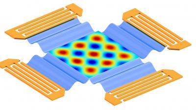
This image shows a simulation of the electric field distribution in a two-dimensionalstanding surface wave field.
(Photo Credit: Tony Jun Huang, Penn State)
In this case, the researchers applied an alternating current to the substrate so that the material's movement creates a standing surface acoustic wave in the solution. A standing wave has node locations that do not move, so the nanowires arrive at these nodes and remain there.
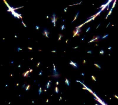
If the researchers apply only one current, then the nanowires form a one-dimensional array with the nanowires lined up head to tail in parallel rows. If perpendicular currents are used, a two-dimensional grid of standing waves forms and the nanowires move to those grid-point nodes and form a three-dimensional spark-like pattern.
"Because the pitch of both the one-dimensional and two-dimensional structures is sensitive to the frequency of the standing surface acoustic wave field, this technique allows for the patterning of nanowires with tunable spacing and density," the researchers report in a recent issue of ACS Nano. The nanowires in solution will settle in place onto the substrate when the solution evaporates, preserving the pattern. The researchers note that the patterned nanowires could then be transferred to organic polymer substrates with good accuracy by placing the polymer onto the top of the nanowires and with slight pressure, transferring the nanowires. They suggest that the nanowires could then be transferred to rigid or flexible substrates from the organic polymer using microcontact-printing techniques that are well developed.
"We really think our technique can be extremely powerful," said Huang. "We can tune the pattern to the configuration we want and then transfer the nanowires using a polymer stamp."
The spacing of the nodes where nanowires deposit can be adjusted on the fly by changing the frequency and the interaction between the two electric fields.
"This would save a lot of time compared to lithography or other static fabrication methods," said Huang. The researchers are currently investigating more complex designs.

This image displays a close up of a three-dimensional nanowire spark pattern.
(Photo Credit: Tony Jun Wang, Penn State)
Source: Penn State