Research into a recently discovered class of materials shows they have the necessary characteristics to develop ultra-energy efficient electronics. Topological insulators (TI) are three-dimensional materials that conduct electricity on their surfaces, while the interior insulates.
Their surfaces are particularly unique because the motion of the electrons is "protected" by symmetry, meaning electrons will keep moving without scattering even when they encounter defects and contamination.
In fact, electrons on the surface of TIs move so robustly scientists are trying to determine the best way to control or "tune" them in order to use them in next-generation electronics. Until now the only way to change the electronic state was to apply a magnetic or an electric field.
But research led by physicists at the University of Wisconsin-Milwaukee (UWM) has revealed a new method. The team proved that surface conduction on a bismuth selenide TI (Bi2Se3) can be enhanced or destroyed, depending on the kind of stress applied to the material at certain locations, called grain boundaries.
The work was published online March 16 in the journal Nature Physics.
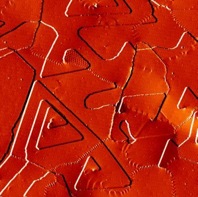
Bi2Se3 is comprised of quintuple atomic layers of bismuth and selenium stacked on top of one another with strong lateral bonds and weak vertical ones between the layers. During its synthesis, when tiny crystalline Bi2Se3 grains coalesce, they form lines of intersection.
These grain boundaries, in which the atoms are either stretched apart or pushed together, can be compared to laying a tile floor starting with randomly placed ceramic pieces, says UWM Physics Professor Lian Li, principal investigator for the National Science Foundation grant supporting the research.

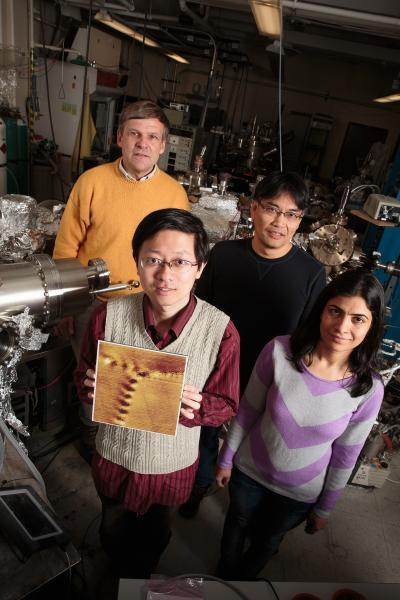
Postdoctoral researcher Yaoyi Li holds an image taken with a Scanning Tunneling Microscope of the 'grain boundaries' on the topological insulator Bi2Se3. Other University of Wisconsin Milwaukee researchers on the paper include graduate student Shavani Rujput and physic professors Michael Weinert (back left) and Lian Li (back right).
(Photo Credit: Peter Jakubowski)
"They do not quite fit together perfectly," says Li, "which produces strain at the joints in the same way as tiles that don't align."
In proximity to a grain boundary where strain exists, the electronic properties on the Bi2Se3 surface are modified. In-plane pulling protects the flow of electrons because the bonds are strong, says Li. Conversely, in-plane compression increases the separation of the quintuple layers, destroying the surface states.
Unraveling the behaviors of TIs is important because it's a promising material for spintronics, an emerging field of nanoscale electronics that involves the manipulation of the electron spin as well as the charge.
By using the orientation of the electron spin, data transfer can be quicker and computing storage capacity increased.
"TIs would work well in spintronics," says Li, "because the spin and velocity of their surface electrons is locked in at right angles."
But first, scientist must find ways to manipulate their behaviors – even to create a simple "on-off" switch.
"So, when we apply compression at the boundaries, then you have no spin movement. All of the sudden, it becomes a switch," says Michael Weinert, UWM Distinguished Professor of Physics and director of the Laboratory for Surface Science. "The advantage here is control. You don't have to apply an electrical field, you can apply stress."

The study found that the atoms are either stretched apart or pushed together at the grain boundaries and that strain can be used to 'tune' the material's unique electronic properties. Here, the boundaries appear dotted or puckered, while the Bi2Se3 grain forms in a triangular shape.
(Photo Credit: None)